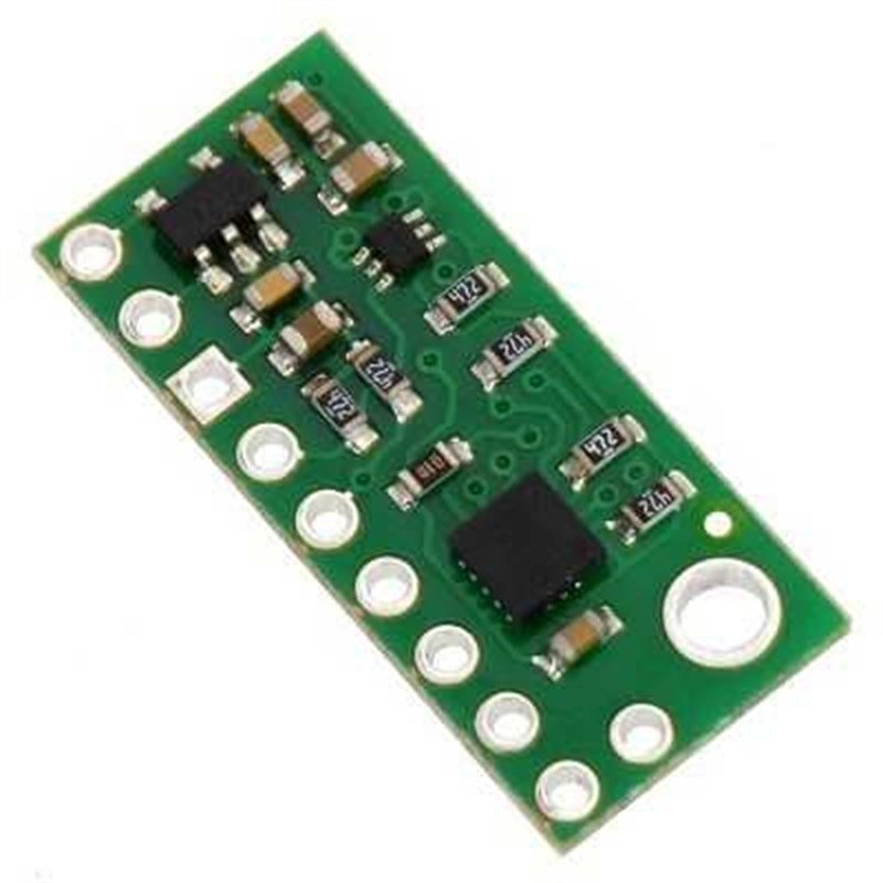
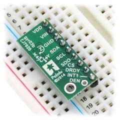
This sensor is a carrier/breakout board for the ST L3GD20H three-axis gyroscope, which measures the angular rates of rotation about the roll (X), pitch (Y), and yaw (Z) axes. Angular velocity measurements with a configurable range of ±245°/s, ±500°/s, or ±2000°/s can be read through a digital I²C or SPI interface. The board has a 3.3 V linear regulator and integrated level-shifters that allow it to work over an input voltage range of 2.5 V to 5.5 V, and the 0.1″ pin spacing makes it easy to use with standard solderless breadboards and 0.1″ perfboards.
The L3GD20H has many configurable options, including three selectable angular rate sensitivities, seven selectable output data rates, seven different embedded FIFO modes for buffering output data, and a programmable external interrupt signal. The three angular velocity readings are available through a digital interface, which can be configured to operate in either I²C or SPI mode.
- Output Format (I²C / SPI) : One 16-bit reading per axis
- Operating Voltage: 2.5 V - 5.5 V
- Supply Current: ~6 mA
- Sensitivity Range (Configurable) : ± 245 ° / s, ± 500 ° / s or ± 2000 ° / s
- Dimensions: 13 × 23 × 3 mm
- Weight: 0.7 g
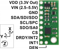
VIN | This is the main power supply connection, and it should be powered at 2.5 V to 5.5 V. The SCL/SPC and SDA/SDI level shifters pull the I²C and SPI bus high bits up to this level. |
GND | The ground (0 V) connection for your power supply. Your I²C or SPI control source must also share a common ground with this board. |
VDD | Regulated 3.3 V output. Almost 150 mA is available to power external components. (If you want to bypass the internal regulator, you can instead use this pin as a 3.3 V input with VIN disconnected.) |
SCL/SPC | Level-shifted I²C/SPI clock line: HIGH is VIN, LOW is 0 V |
SDA/SDI | Level-shifted I²C data line and SPI data-in line (also doubles as SDO in 3-wire mode): HIGH is VIN, LOW is 0 V |
SDO | SPI data-out line in 4-wire mode: HIGH is VDD, LOW is 0 V. Also used as a 3.3V-logic-level input to determine I²C slave address (see below). This pin is not level-shifted and is not 5V-tolerant. |
CS | SPI enable (chip select). Pulled up to VDD to enable I²C communication by default; drive low to begin SPI communication. |
DRDY/INT2 | Data ready indicator, a 3.3V-logic-level output. HIGH (3.3 V) indicates angular rate data can be read. Can also be configured as a FIFO interrupt. This output is not level-shifted. |
INT1 | Programmable interrupt, a 3.3V-logic-level output. This output is not level-shifted. |
DEN | Data enable trigger, a 3.3V-logic-level input. This input is not level-shifted and is not 5V-tolerans
|


